Strategic U.S. Expansion for HBM Leader
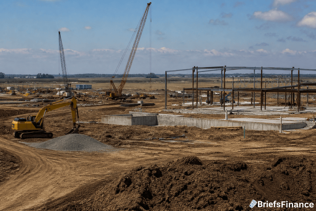
SK Hynix has commenced building a $4 billion advanced packaging plant in Indiana to address booming demand for high-bandwidth memory used in artificial intelligence systems. During the August 2026 groundbreaking, company leadership highlighted the facility's role in diversifying global semiconductor supply chains.
Kwak stated, "This will transform Indiana into America's premier HBM manufacturing location," with the initial production cleanroom slated to open by late 2028. The project aligns with SK Hynix's $720 billion worldwide investment strategy to maintain its lead in the competitive memory market.
Packaging Specialization Amid Manufacturing Debates
While U.S. officials have urged semiconductor companies to establish complete fabrication plants domestically, SK Hynix's Indiana facility will focus solely on packaging and testing chips manufactured at its Asian facilities.
The CEO noted the company continues evaluating options for potential future U.S. wafer production. Located near Purdue University's engineering programs, the site offers access to technical talent while strengthening North American supply chains for critical AI components.
Markets move every day, and most of it never reaches you in time. Get the free Market Briefs daily newsletter and stay ahead of it.
Addressing HBM Bottlenecks
The Indiana plant specifically targets production constraints for high-bandwidth memory packaging, which has become essential for AI accelerators. Currently, nearly all HBM assembly occurs in South Korea, making this the first major U.S. facility dedicated to advanced memory packaging processes.
State officials and academic leaders joined SK Hynix executives at the groundbreaking, emphasizing the project's role in America's semiconductor ecosystem. The investment reflects how memory manufacturers are adjusting their global operations to meet AI-driven demand while addressing geopolitical supply chain risks.
Background on HBM's AI Importance
High-bandwidth memory has emerged as a critical component for AI servers, with its stacked design enabling faster data transfer between processors and memory. SK Hynix currently dominates the HBM market alongside Samsung, supplying chips to major AI hardware developers. The Indiana facility will help alleviate bottlenecks in packaging capacity that have constrained shipments amid surging demand for AI infrastructure.
For semiconductor investors, SK Hynix's expansion highlights the intensifying competition in memory technologies powering artificial intelligence applications. The company's multibillion-dollar global buildout positions it to maintain technological leadership in this high-growth sector while establishing crucial U.S. production capabilities.